Listen, anyone can make a PCB at home, it’s easy. PCBs (printed circuit boards) are those flat things with all the components that are inside all electronic devices, you’ve seen them. All you need is a laser printer, some glossy magazine pages, print your circuit onto the page, use a clothes iron to transfer the toner onto your copper clad, if that doesn’t work use some water and some lacquer or something, I don’t know, I stopped reading at that point because the last time I saw a laser printer, a magazine and a clothes iron was in the nineties.
Until recently, the only ways I knew to make PCBs was to practice the dark art above, to pay $10 and wait three weeks to get professional-looking PCBs from China, or to pay $60 and wait three days to get professional-looking PCBs from Europe. It was “cheap, fast, actually doable by a human person, choose two”.
That always bugged me, it shouldn’t be like that, I have always been of the opinion that there shouldn’t be things you can’t make when you have a 3D printer, but PCBs have consistently eluded me. I yearned for them, I wanted to be able to make them at home, but it seemed impossible.
One day, everything changed.
That one day when everything changed
One day, I thought it would be fun to mount a pen onto my 3D printer and got it to draw stuff (penises) on paper. If you don’t know how a 3D printer works, now would be a good time to skim my 3D printer primer, but in summary a 3D printer cuts an object into 2D slices and prints them on top of each other.
If I could take just one of these slices and tell the printer to print higher, then the nozzle wouldn’t be touching the bed, I could mount the pen lower and put a piece of paper under it, and it would draw on the paper. Getting the printing software (called a slicer) to create a 3-dimensional shape out of a photo was easy, as you can just import a drawing and it will automatically convert it to a solid.
I rubber-banded a Sharpie onto a holder I quickly designed, and, a few lines of code later, my printer produced this gem (excuse quality of potato):
I felt so proud of the completely useless thing I had created, I immediately ran to share it everywhere. A friend saw it on Twitter and replied that this was a good way to make PCBs.
I was immediately intrigued.
Making PCBs with markers
Apparently, all that black magic about printing and transferring and magazines and lacquer above is just a way to keep the etching acid from dissolving the copper. You see, when you’re etching a PCB, you’re basically getting acid to dissolve the copper on your copper clad (the blank PCB). Except, you’re putting something (toner) over the copper on the parts you want to keep, so the acid can’t get to it, which leaves you with copper traces.
It turns out you don’t really need to do all that stuff with the toner and printer, since you can cover the copper much more easily just by drawing over it with a permanent, waterproof marker (I used an Edding 140 S 0.3mm). I had inadvertently created a plotter, which can be used for painting a circuit onto a PCB.
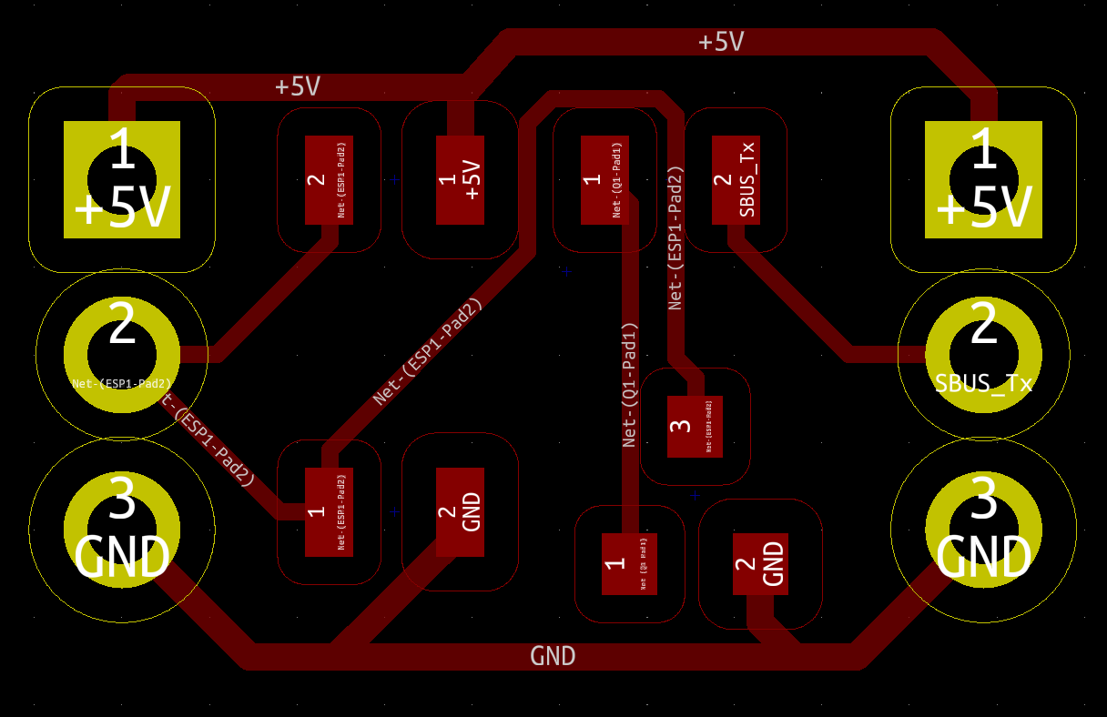
I rushed to dig out the files for one of my old, small PCBs, which you can see on the right, and ran it through my improved drawing process. I had the printer draw it on paper, just to see what it would end up looking like, and the results were pretty encouraging.
The paper somewhat absorbed the ink, as paper is wont to do, so there was some seepage, but overall the results looked like they should definitely work on copper. This is that first attempt:
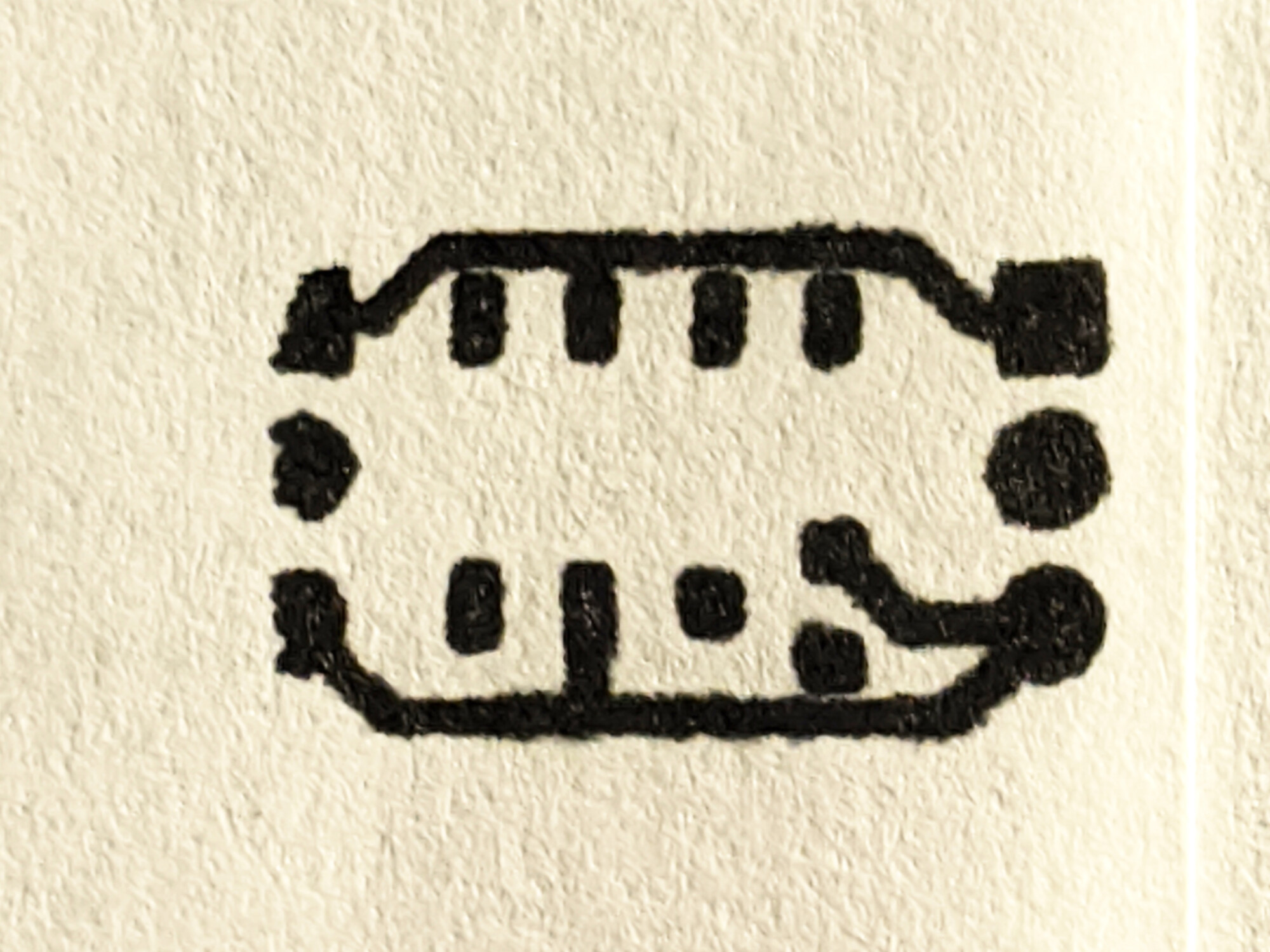
This looked very promising.
The improved drawing process
The original process (where I exported stuff to an image and then converted the image to a 3D model with the slicer) worked well enough, but it was meant for working with 3D models, not circuits. As such, it could sometimes lose accuracy, which doesn’t really matter if you’re printing a figurine, but does matter if it means your circuit is no longer working.
Fortunately, there is an excellent open source project called pcb2gcode, which converts Gerber files (Gerber files are basically files that describe your PCB so the fabrication factory can make it) to Gcode for various CAD tools to execute it. The Gcode that pcb2gcode outputs wasn’t compatible with my Marlin-style printer, so I adapted my script from above to turn the output to something my printer can run.
My script does various things:
- It removes commands that are incompatible with or unsafe to run on my printer (e.g. drilling commands, as it has no drill, temperature and extrusion commands, as I don’t want it to heat up or extrude, etc).
- It rewrites comments so that they are compatible with my printer (pcb2gcode comments use parentheses, my printer uses semicolons).
- It makes sure all movements are within some specified coordinates, so the print head can’t go too low or too high by mistake.
- It allows me to offset all drawing commands by some distance, so I can print exactly where I want to.
Unfortunately, as you can see on the photo of the paper drawing above, pcb2gcode has a bug where traces that are too narrow disappear, but the author is actively working on it and I worked around it in the mean time just by setting a lower marker tip diameter.
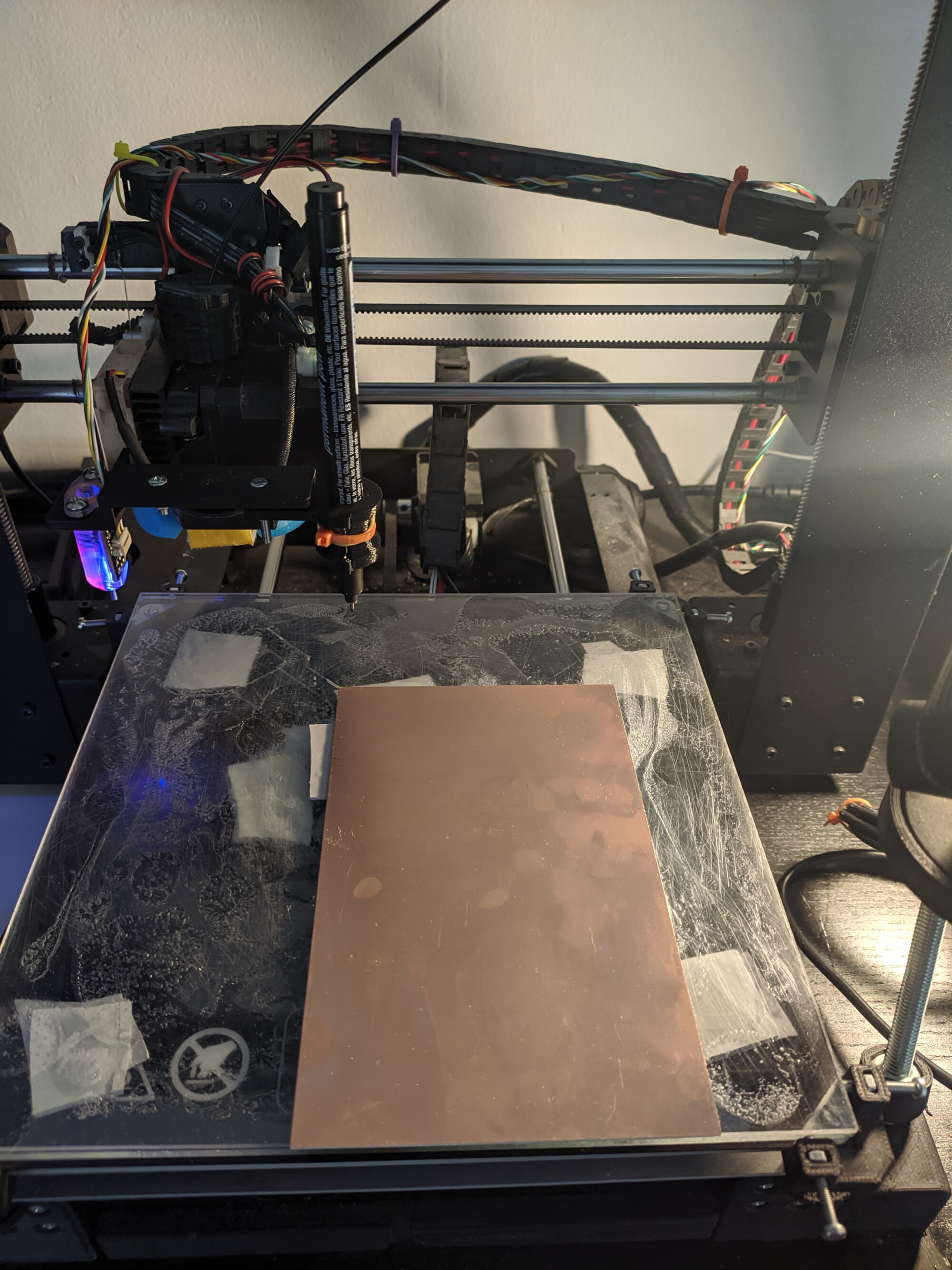
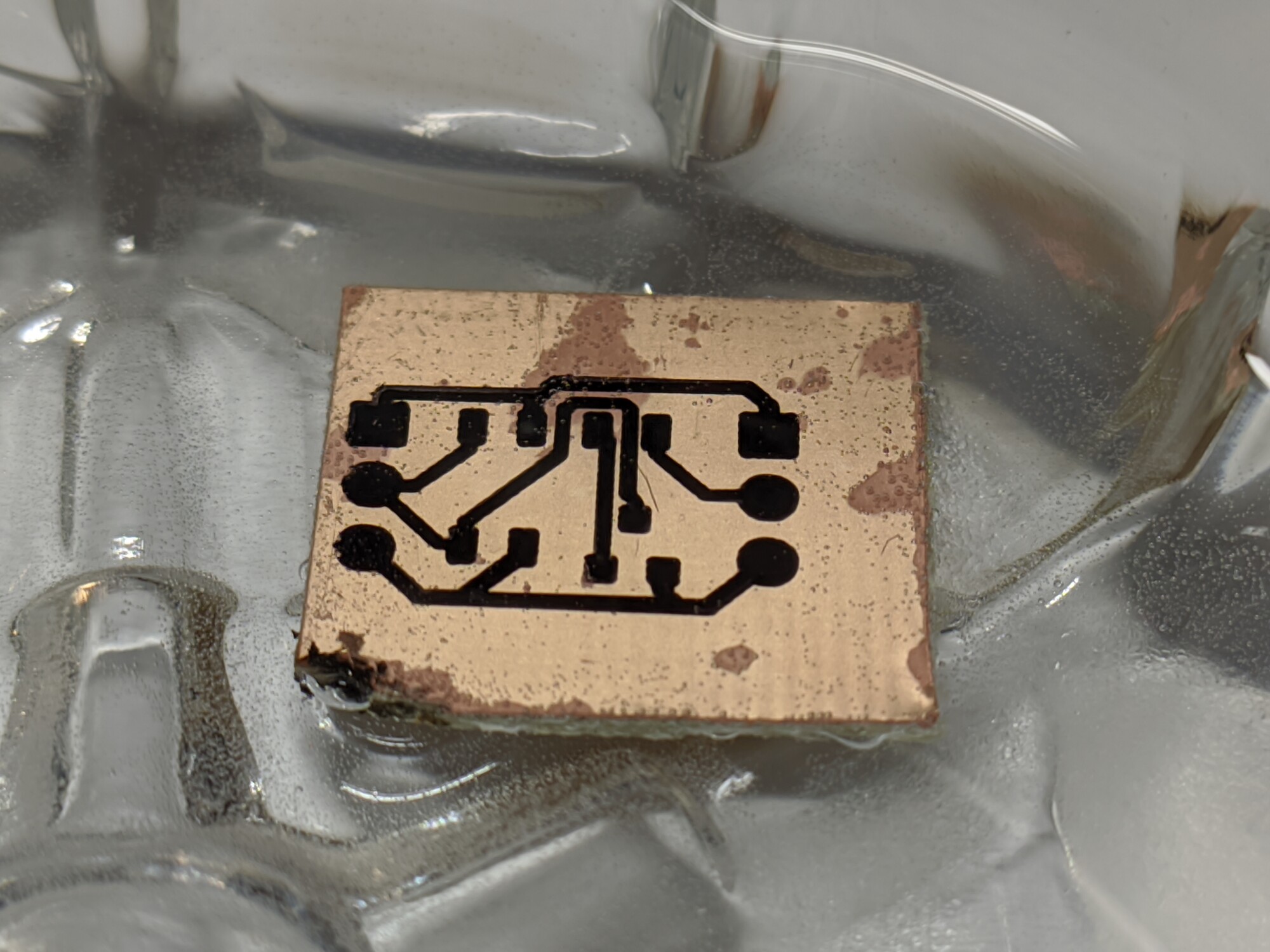
Once everything was done on the programming side, and with lots of help from my friend Andrew, it was time to actually try and draw on copper. Here’s a video of the attempt:
As the copper isn’t porous, the drawing looks much better than on paper. The traces are very accurately drawn, though the tolerances are a bit too tight for my liking. One trace at the top, especially, is way too close to the pad, though they aren’t actually touching. I’d have to see whether they would be bridged after etching, though.
You also might notice a small hole in the very first pad, that’s because the ink hadn’t started running yet. It was easy to fix by just painting it in with the marker at the end.
The only thing left to do is take some of that copper layer away so we’re left with our traces.
Etching
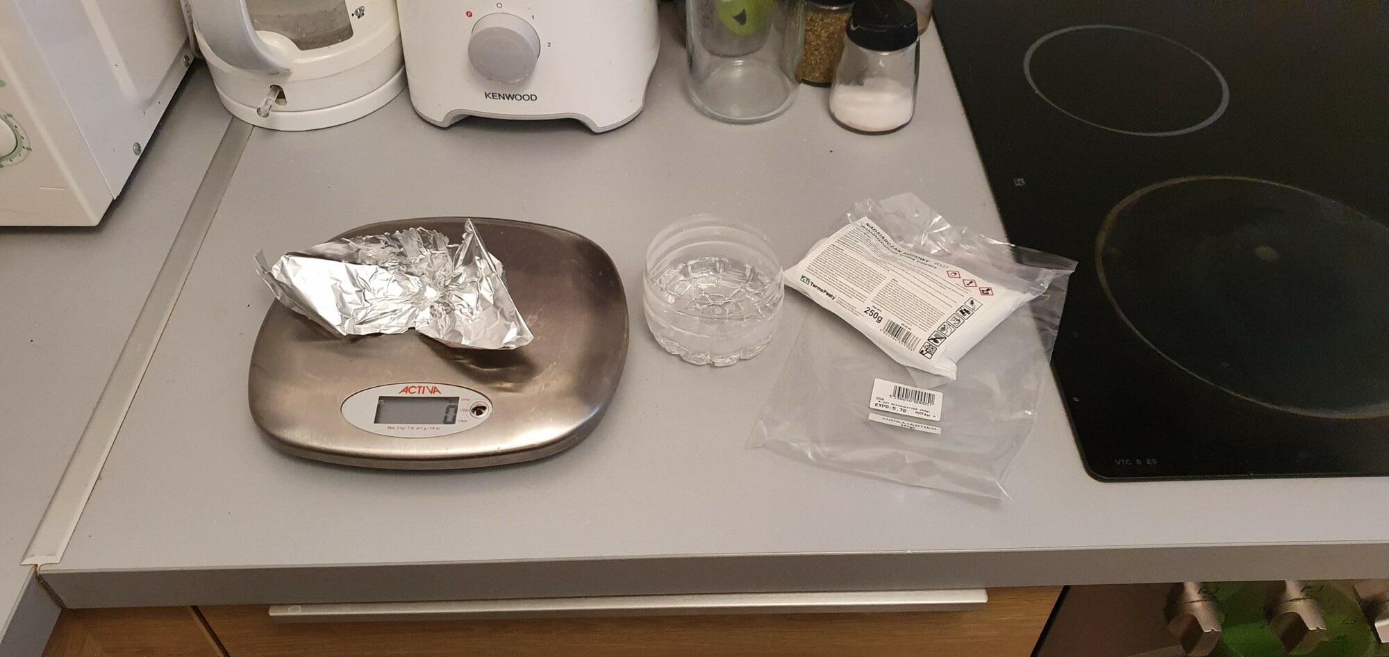
Surprisingly (and as my friend Josh rubbed in with what I imagine to be considerable glee), the actual etching part wasn’t as easy as I thought. It wasn’t hard, but it also didn’t consist of just throwing the PCB in acid and waiting.
I’m still in a trial-and-error phase, as I’ve only etched two PCBs, but it seems like 100 grams of water with the appropriate amount of sodium persulfate dissolved in it is only good enough to etch a tiny PCB. If that’s true, it will take a lot of acid to etch a larger one, but I’ll have to experiment and see what happens.
UPDATE: Some commenters on HN pointed out that the reason this took so long was that I didn’t have a copper plane. I decided against that initially because I didn’t want the marker to have to basically paint the entire PCB, but after having etched, it’s definitely worth it. A plane makes it so that a lot of the copper is left on the PCB, and only the outlines of the traces are etched, which is all you need anyway. This way you aren’t wasting your etchant trying to etch a lot of copper, it takes less time, and your PCB ends up better etched.
The other thing I’ve learned is that you shouldn’t heat the water above 50ish C, otherwise it starts to vapor and that can’t be good for anything.
Also, the first time I etched a PCB I kind of just left it in the acid, but it turns out the copper dissolves much faster if you’re agitating or stirring the mixture. I started looking into designs for building an agitator for subsequent tries, but then realized that you don’t need one if you have a 3D printer, and wrote this Gcode file instead:
It even heats the bed to 40 C so your etchant is kept warm! Is there anything 3D printers can’t do? Doesn’t look like it!
Etchant health concerns
I have no idea what the health concerns for these chemicals are. I’ve kind of just tried to avoid getting too close to the vat, even going as far as to put the lid on the tupperware container I was using, but I don’t know whether that delays or somehow impedes the etching process.
It’s been hard to find info about all these chemicals, so if you know anything, please leave a comment below or send me an email, especially if you know of a better/more convenient/safer etchant. I will update the article with any info as it comes, for the edification of anyone who reads this.
UPDATES:
throwanem on HN says that sodium persulfate isn’t too bad, the biggest problem is fumes which can be kept to a minimum at low temperatures. Higher temperatures accelerate the etch, but the fumes shouldn’t be inhaled. It’s also a fire risk, and should be kept cool and dry.
As always, any etchant should be safely disposed of and not poured down the drain.
The etching continues
Etching was otherwise uneventful, the PCB started bubbling at some point and then it started flaking, and the etchant turned slightly blue, which I assumed meant it was working. Agitating it a bit made it flake more, which seemed like a very good sign, so I just kept doing it and it kept working. I then left the mixture to its own devices because I was getting bored, until I noticed it was finally done.
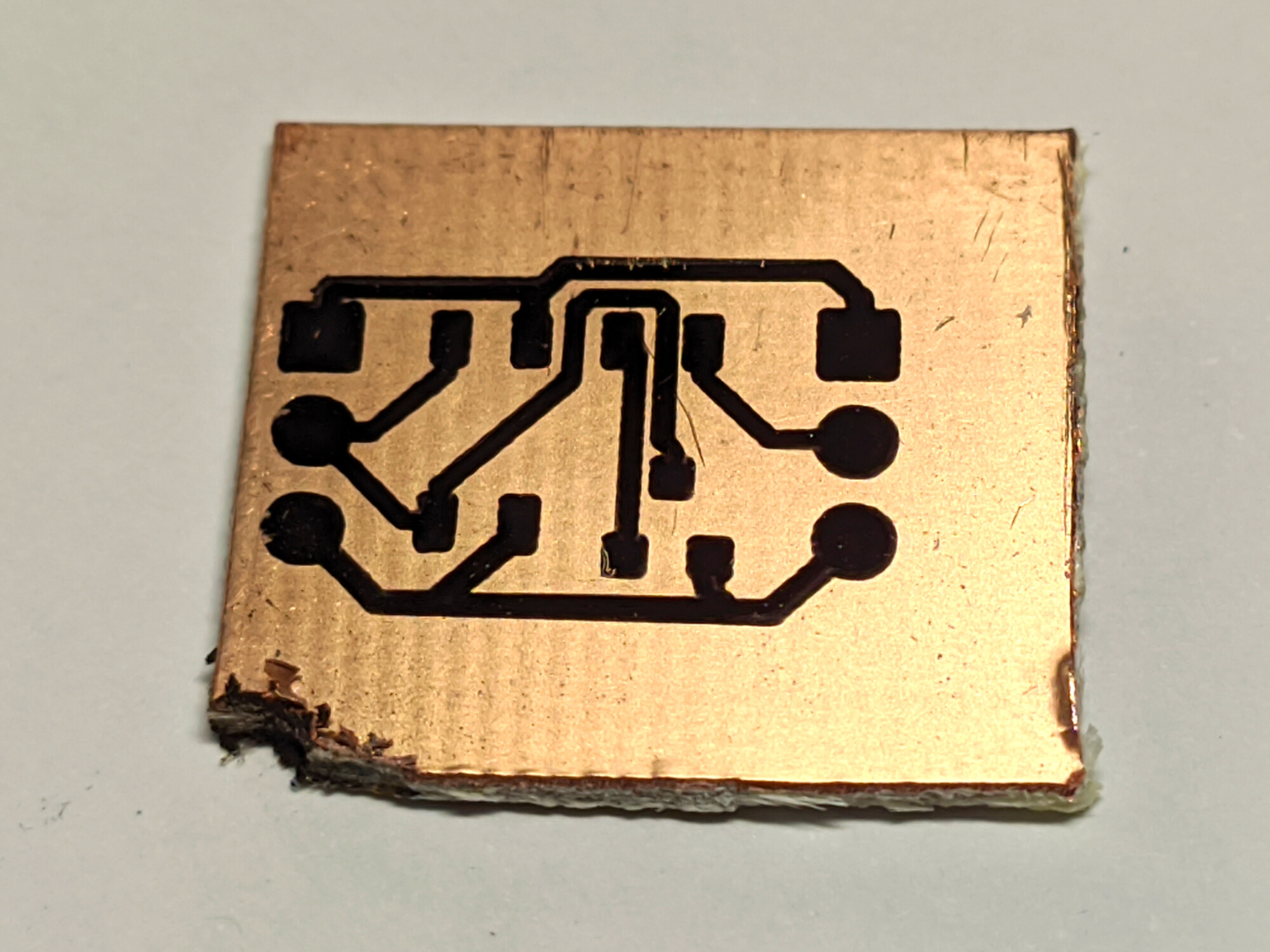
Eventually I was left with a slightly over-etched but otherwise extremely respectable PCB. I don’t know why the over-etching happened, I imagine it was because I left it in the etchant for half an hour. Maybe I need to use more etchant for it to go faster and not have time to over-etch, I hear it should ideally take from three to ten minutes.
Regardless, with no small amount of pride, here’s my first ever home-etched PCB!:
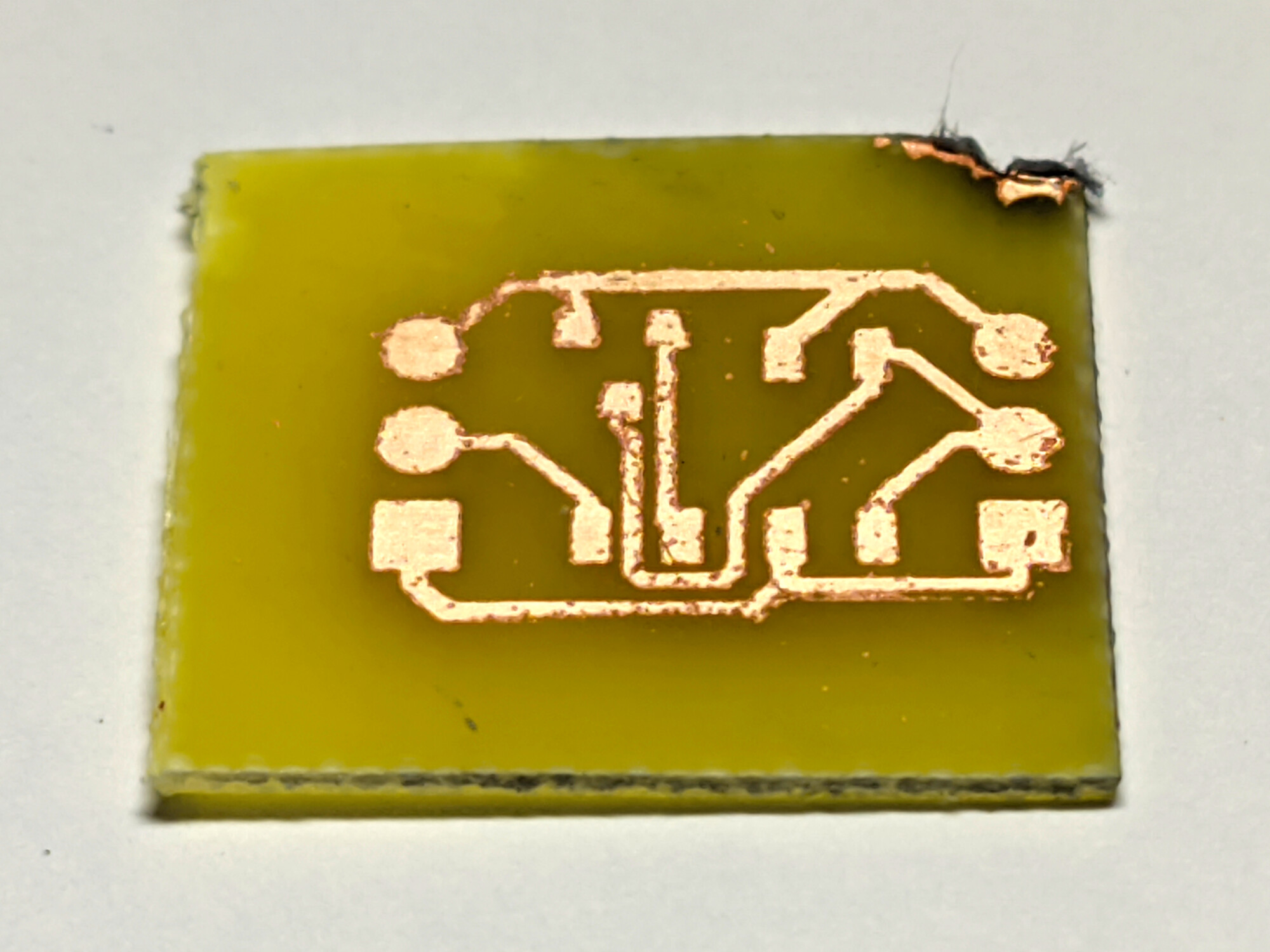
It both looks good and works well! I tested everything with the multimeter and everything that should be connected is connected, and nothing that should be disconnected isn’t disconnected.
All in all, I would call this an unconditional success!
This was all a ploy
Of course it was a ploy! What did you think, that I spent all this time, effort and tax payer dollars to create a signal inverter for an RC airplane? Don’t be naive.
My ultimate goal was far more nefarious, and with Andrew’s help my life-long dream is now a reality. I present to you this:
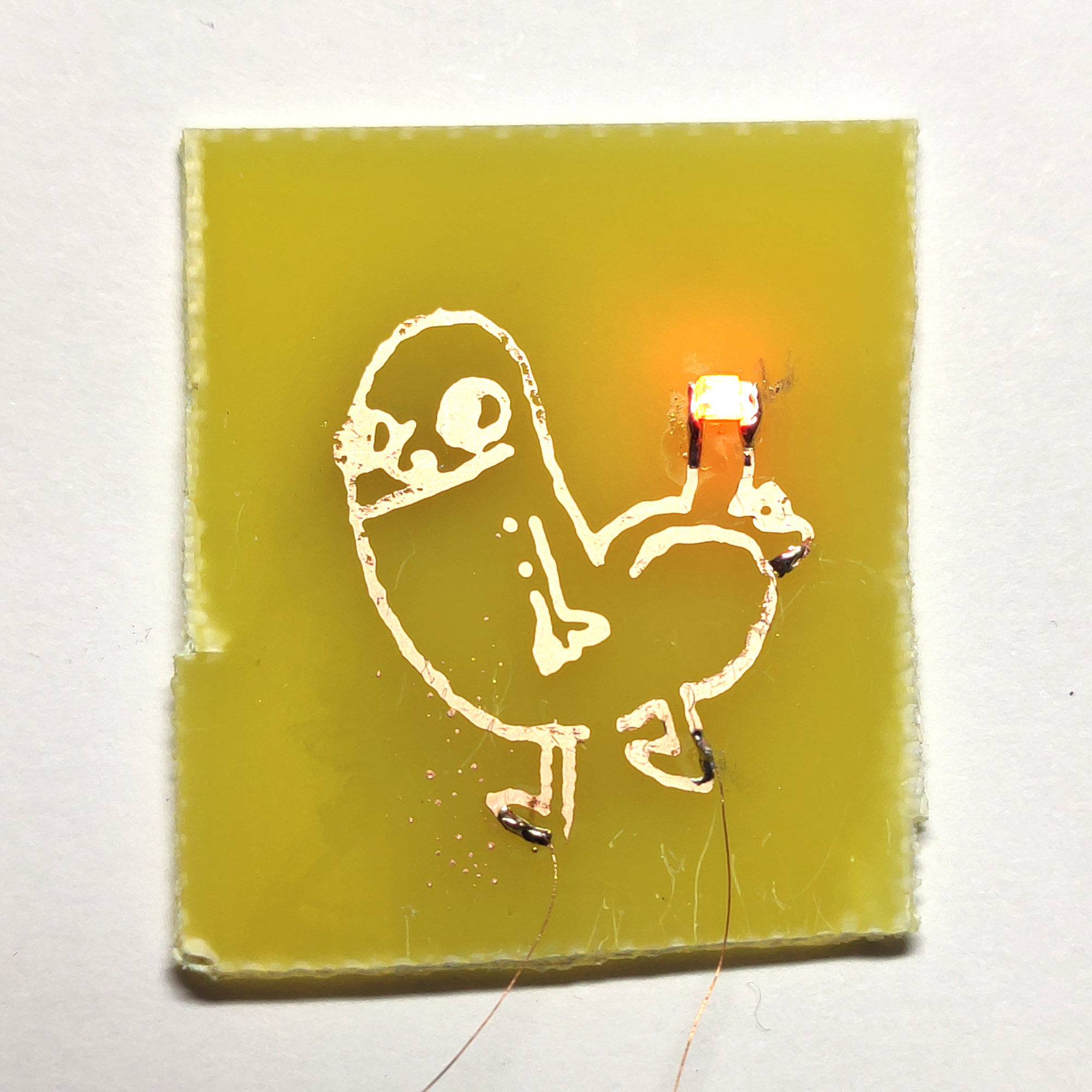
Yes, that is a dickbutt PCB with a red LED on the dick on its butt.
If you don’t know whether to laugh or cry, you are exactly right, because that’s precisely what I was going for.
Epilogue
I am extremely excited about this process, as it finally allows me to easily make PCBs at home, quickly, conveniently, cheaply and at rather high tolerances, for what it is. I have been looking for something like this for ages, and I really think it could spark a minor revolution with hardware enthusiasts. It’s definitely much faster, better, more fun and more convenient than soldering protoboards, which I hate hate hate.
If you want to do this at home, all my code, Gcode files and process documentation are in this repository:
https://gitlab.com/stavros/pcb-plotting
Feel free to open an issue if something isn’t working properly, or a PR if you want to improve something. I’d appreciate your help.
Also, as always, please Tweet or toot at me, or email me directly.